Reproducing the HP 8601A Output Hybrids (5086-7112, 5086-3012, 1820-0150)
I have succeeded in making reproduction HP 8601A output amplifier hybrids which match or exceed the performance of the original parts. For those curious about the process, read on!
First a bit of background. The story really starts with another project, reproducing the HP 1820-0285 ICs for the 8007 series pulse generators (see my blog post here). After I finished that project I was really excited about the prospect of applying my skills to other obsolete / NLA ICs especially ones with broader appeal, as the 1820-0285 is really obscure. I have been interested in the possibility of reproducing the output amplifier for the 8601A for several years, ever since I read a post on the Antique Radio Forum (http://www.antiqueradios.com/forums/) asking for a replacement, so when I was contacted by Antique Radio Forum member bkharris about fixing a pair of HP 8601A sweep / signal generators I gladly accepted.
After receiving the generators, I did some troubleshooting and discovered that the attenuator was blown in one, and it also had a bad output amplifier hybrid. The other one had a bad preamplifier hybrid but a good output attenuator and output hybrid, thus giving me a good set of hybrids for bkharris, and a pair of bad ones for me to try reverse-engineering. Furthermore, bkharris was extremely kind and donated the parts of the bad sweeper to me so I would have a testbed for the new hybrids. He also very kindly allowed me to hold on to both sweepers for about three months while I finished development of the hybrids (and finished repairing the good sweeper, although that is another story all together…) I owe him a HUGE THANKYOU for making this possible!
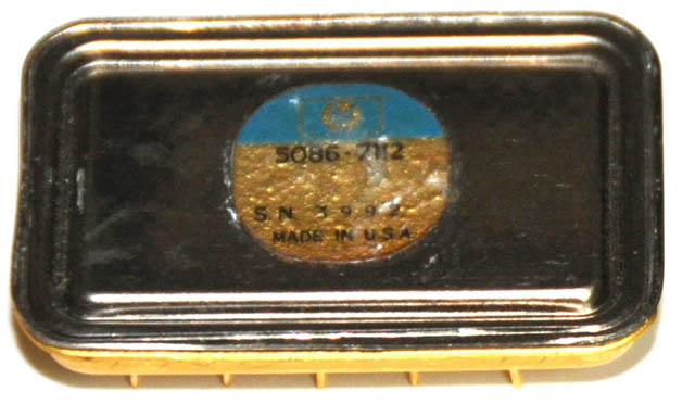
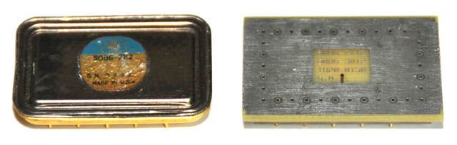
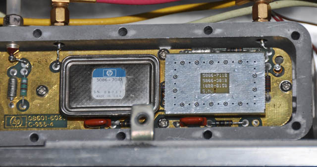
O.K. Now onto the actual project. For those of you who haven’t yet gotten a chance to venture into an 8601A, the output hybrid is a little gold can as shown below. The one I reverse-engineered is marked 5086-7112, but the part was also sold under the part numbers 5086-3012 and 1820-0150.
The top of the can is welded onto the bottom, so the first challenge was getting the darn thing open without destroying the very delicate circuity inside. I finally accomplished this by using a razor blade as a tiny saw to cut through the soft gold and copper of the seam in one corner. Once I penetrated the corner, I was able to work the razor blade along the seam and slowly separate the weld. Once I got it open, I used a microscope to create a mosaic of pictures and then I stitched these together into the composite shown below.
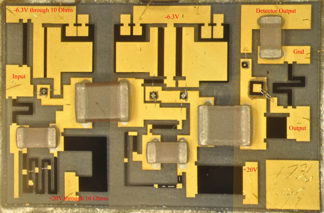
As you can see, the device consists of a sapphire substrate with thin-film resistors deposited on it. (Thanks to K7KSW for correcting me on the substrate material.) On top of this, ceramic capacitors were soldered, and discrete bare-die silicon devices were attached and wire-bonded. Finally, the whole unit was adhered to the bottom of the can and wire bonded into place before the lid was welded on.
From the pictures, It was easy to determine that three of the devices were transistors and one was the detector diode, but the final silicon device proved a mystery. It looked like a diode, but measured the same conductivity in both directions, and since it was connected across the output resistor, it didn’t make much sense for it to be a diode. After much simulation and experimentation I eventually determined that it was a MOS capacitor which serves to flatten the output by reducing the impedance of the output resistor at high frequencies and thus compensating for high frequency attenuation elsewhere in the circuit. Also note the wire bond jumpers which serve to adjust the values of what I am calling R3 and R8, and thus set the bias of the transistors.
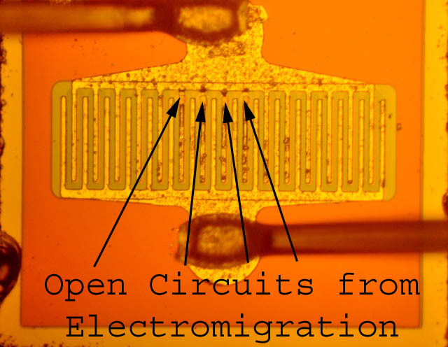
Before proceeding the the actual reverse-engineering, out of curiosity, I used a high power microscope to examine the transistors, looking for the original failure. Sure enough, one of the transistors in the output stage showed an absolutely text-book electromigration failure. (Electromigration is a process by which metal gradually moves away from areas of very high current density to areas of lower current density, eventually causing failure by open circuit.) The picture below shows the failed transistor.
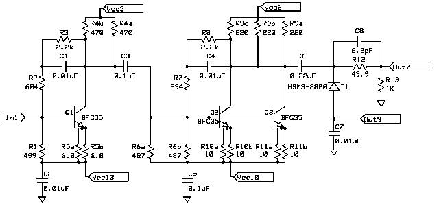
I then proceeded to trace out the circuit, measure all the capacitor values (except the MOS capacitor) using an impedance analyzer, measure the values of all the resistors, and create the schematic below. This was easier then the 1820-0285 as the circuit is much simpler, but also more challenging in that, being an analog circuit, resistor values were much more critical. After discovering that resistors with the same dimensions measured radically differentially, I ended up calculating the values of all the resistors based on their W/L ratios and the resistivity of the thin-film material which I calculated from the value and dimensions of the output resistor, which I was pretty sure was 50 Ohms. I then compared the calculated values to the measured values and compromised appropriately, aided by an LTspice simulation. Also note that the schematic shows several resistors as parallel combinations of multiple resistors more on this later, but in the original each of these was implemented by a single resistor.
Armed with this deceivingly simple schematic, I then set about designing a mechanical package which would fit in place of the original hybrid and laying out a board which to reimpliment the circuit. The package that I devised is shown later in this post, but the hardest part of designing it was finding appropriate pins. I ended up finding a Mill-Max part that works, but it was only available from Mill-Max themselves, not from any distributer. Luckily, though, I was able to get a sample, but once those run out I don’t know what I am going to do. The main challenge with the board was that the collector resistors dissipate over a watt of power each! I couldn’t actually fit 1W resistors in the tiny package, so I used multiple 0.5W 1210 package parts in series to implement the collector resistors. The other challenge was find appropriate transistors. They also needed to dissipate about a watt of power and have a transition frequency on the order of 1GHz. Fortunately, I found that BFG35 parts fit the bill. The board I designed at this point is shown below.
After building it, the first step was to choose values for R3 and R8 (which were hand-tuned in the original) to get the right bias current. After a bit of experimentation I chose 2.2K resistors as this biased the transistors with slightly more current then my good working output hybrid, but less then the bad ones which I took apart, while keeping all the parts under their rated power specification. Unfortunately, upon powering it up in the 8601A, the output meter pegged and could not be reduced with the output vernier knob and there was, apparently, no output. It appeared as if the circuit was oscillating, as the detector was putting out several volts independent of input, but I couldn’t see any oscillations on either my 400MHz oscilloscope or the 1200MHz spectrum analyzer. Very puzzled and annoyed that I had apparently wasted money on a run of boards, I put the project aside. When I got back to it, I had the realization that it could be oscillating above 1200MHz! Sure enough connecting it to the microwave counter revealed a ~2GHz oscillation! By hacking in a couple of emitter bypass capacitors I was able to quench it and discover that, otherwise, the circuit worked nicely!
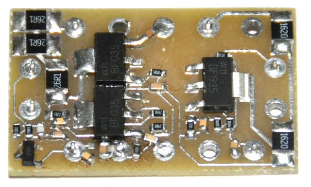
Thus, with renewed spirit I designed a second board. This time, I was extremely careful to keep inductances low. I used large plains of metal rather then traces whenever possible and put the collector resistors in parallel instead of series. The result, shown below, is quite pretty, if I do say so myself. I also found 0.75W 1210 resistors which gave me a nice bit of safety margin.

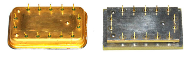
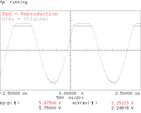
This revision worked on first power up, and after tweaking the output resistor bypass capacitor (C8) it actually proved to be flatter then the original, at least by my power meter! It also has about 3dB more gain then the original, easily meeting the 22dB specification. The picture below shows the completed product, both top and bottom, next to the original.
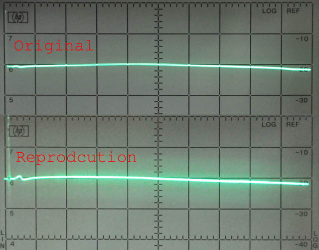
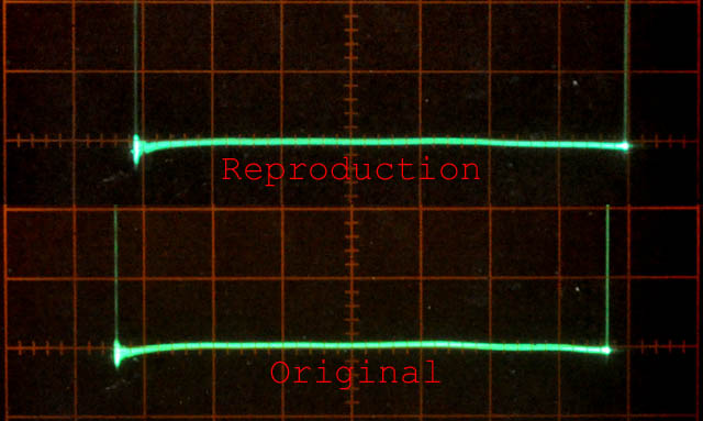
Testing of the open-loop flatness revealed, that aside from a small low-frequency bump, it was as good as the original. Results are shown below.
Furthermore, testing the flatness with an RF detector reveals that, even under the fastest sweep rate, it is just as good as the original. Note that the droop at low frequency is due to my RF detector not being good below about 10MHz.
Finally, I checked the harmonic content per the original manual and found it to be equal to or superior to the original across the entire band. Furthermore, there is less clipping at high output. Note that these units always clip at +20dBm into 50Ohms. From the original HP service manual “…noticeable distortion will almost always be present at some RF output frequencies with output levels above about +16dBm.” However, my reproduction shows less distortion, and more symmetric distortion, then the original.
Thus, I will call this project done! You can buy the reproduction parts here.
Depending on the availability of the pins, and community interest, I plan to reproduce the preamplifier hybrid (which is also used as the loop amp) shortly. When that is done I will be able to put the bad sweeper that bkharris so kindly donated back together. Once again THANKS A MILLION to bkharris.
Here it is installed:
As far as I know this hybrid was used only in the 8601A sweep / signal generator, but I would love to hear about it if anyone finds another application.
-Matthew D’Asaro
Hi Matthew, I have an HP8640b and a HP 8601a and the 8600a marker generator that goes with so I was very interested in your article on rebuilding the power o/p device in the 8601a.
I realise it has been a number of years since you posted the article but I was wondering if you made up any of these boards for sale,also how it stood up over time.
In any event thank you for a very well written and illustrated piece on your project.
Frank King VE1FEK
Thank you very muchf for the comments! I am glad you enjoyed my article. My replacement hybrids are availible for sale to the world on eBay. Just search eBay for ‘8601a hybrid’. As far as long-term reliability goes, I have sold over a dozen of the parts to people all over the world and no one has reported a failure. Aside from that and that they were designed so as to keep all parts within their maximum operating ratings, I have no solid data on longterm relability.
Hi Matthew,
I wonder if I can still purchase the re-engineered HP 8601A hybrid amplifier?
Thanks,
Mike
Sorry. I am closed until March. I am moving cross-country to Seattle after finishing my PhD at MIT. I will let you know when I am setup again on the other side.
-Matthew
Hi Matthew,
Are These amplifiers still available somewhere?
Kind regards,
Gottfried
Sorry. I am pretty much out of business for the foreseeable future. I no longer have my lab setup after I moved to Seattle to take a new job and don’t have the time to work on this stuff either. Good luck with your project.
-Matthew D’Asaro
Great article and, wow, impressive reverse engineering perseverance. Nice job.
My E2 (70112) amp is working but the detector output is zero. I’m going to try tacking an external diode detector outside the package.
Hope that job of yours in Seattle worked out for you.
Regards,
Retired Watkins Johnson Company engineer here in Oregon.
Thanks so much for the compliments and congrats on getting your unit fixed. In case you are curious, I am really enjoying my work at Sea-Bird Electornics (www.seabird.com)
-Matthew D’Asaro
As I said in earlier post that didn’t get listed for some reason: Really nice reverse engineering!!
My 7112 has an internal detector diode failure. I was able to kludge repair it by using a 1n4148 diode. Lift the end of the 12k resistor inside the video amp housing that goes to the hybrid. Solder the banded end of the diode to the RF output pin and the other end to the lifted 12K resistor.
To test to see if your internal diode is bad, disconnect the coax to the detector output connector. Remove vid module cover. Set generator to +20dbm output. The detector output at the vid module output pin should be between -3 and -4 volts. If 0 or ~-1 volt then detector not working and the above may fix it.
Thanks so much for the compliments and congrats on getting your unit fixed.
-Matthew D’Asaro
Thanks for posting and glad you’re still around.
Error in my above post:
“Lift the end of the 12k resistor” SHOULD READ: “lift the end of the 3480 ohm resistor that goes to the hybrid. Solder the banded end of the diode to the RF output pin and the other end to the lifted 3480 ohm resistor”
(sorry for the error)