Reverse-Engineering an IC to fix an HP 8007A Pulse generator
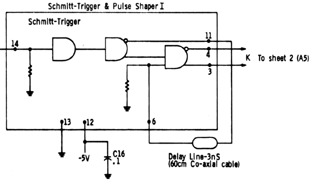
Well friends, I have another test equipment repair story to share, this one the most advanced that I have done to date. However, let me apologise in advance for the length of this posting. The story begins in 2007 when I, as a freshman at UW, bought a broken HP 8007A pulse generator on eBay for cheap figuring that it would be an easy fix. The problem was absolutely no output so I figured that it was likely just a bad power supply. Hah! Troubleshooting quickly revealed that the problem was likely one of the HP custom pulse-shaper ICs (P/N 1820-0285). Per the diagram below, these chips consist of ECL logic gates and are used to shape a pulse to a specific width controlled by a delay line.
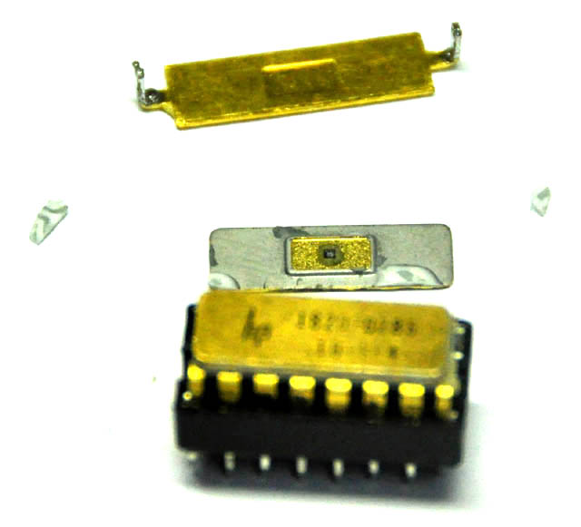
Anyway, I went to unsolder the chip so I could breadboard test it. I unsoldered all the connections but I didn’t have my nice vacuum desoldering system yet so I didn’t get all the solder out. Annoyed that it wouldn’t lift out, I tried prying. Crack! The ceramic and metal IC package delaminated, tearing off all the bond wires. Oops. The picture below shows the heatsink which delaminated from the bottom of the chip, the bottom layer of the package with the die on it, the top of the package with the leads, and several small chips of the ceramic material that held them together.
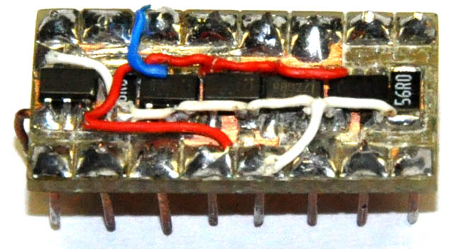
Not knowing much electronics at that point, I looked at the block diagram and thought: ‘oh this chip is made of logic gates. I bet I can make a replacement by wiring up discrete logic gates!’ Not understanding the differences between logic families, I chose Fairchild TinyLogic gates, which are fast CMOS (and therefore doomed my plan from the start as CMOS is completely incompatible with ECL.) Not knowing this I blissfully went ahead to layout a custom ‘PCB’ in Rhinoceros (3D Modeling software), printed out my design, pasted it to a piece of copper-clad FR4 and then used a razorblade to make the board. I used wire wrap wire to make flying connections for power and ground and wala I had the replacement ‘chip’ pictured below. Naturally, though, it didn’t work at all. Frustrated, I put the project aside.
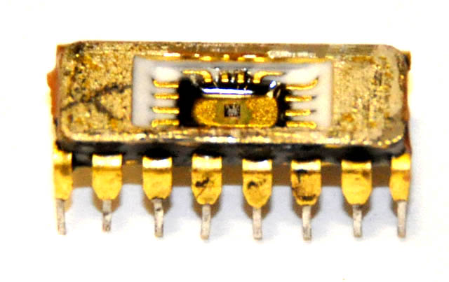
Fast forward five years to 2012. I am now at MIT and have access to a complete semiconductor lab so I figured I would give a try at repairing the chip package so that I could see if the IC was actually bad or not. To this end, I used my hot-air rework station to remove the brazed-on lid of the IC and then I used MG 832HT epoxy to re-laminate the bottom metal layer which holds the die, to the ceramic middle portion that holds the leads. Amazingly, this worked almost perfectly and resulted in the reconstructed device shown below. Note that the lid is removed to facilitate wire bonding.
I then ‘just’ had to wirebond it back together. I tried doing this myself, but all I managed to do was lift some of the bond pads because the wire in the bonder was too big. I though it was all over, but then a friend of mine was able to get it bonded by a more skilled operator working a better machine and I could finally test the chip! With shaking hands I powered it up and… No dice. Not only had one of the bond wires not taken, it was clear that the chip was blown after all.
At this point I had seen the chip under the bonder microscope and realized that it was not very complicated. Not about to give up, I decided to see if I could reverse engineer the thing! Thus, I used a high power optical microscope to take pictures of all portions of the die. I then combined them in Photoshop to produce a high-resolution die image (shown below.)
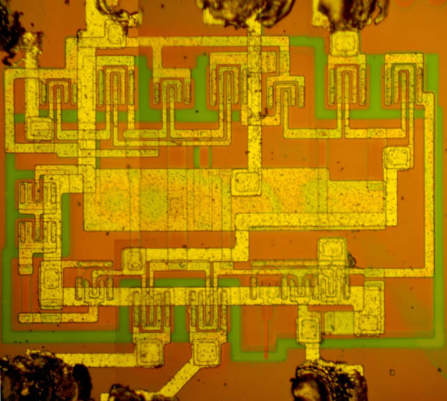
From this die image I was able to work out the circuit topology. Knowing that the input resistor was 50 ohms, I was able to calculate the resistivity of the thin-film material used to form the resistors. Then from the dimensions of the remaining resistors I was able to calculate all their values. I took all this information and produced a complete simulation of the IC in LTspice IV, verifying that I had the circuit drawn correctly and that the resistor values were roughly correct. See the schematic below.

I then laid out a two-layer board in ExpressPCB that fits in the original 16-dip footprint and replicated the circuit topology exactly using SOT-23 transistors and 0603 resistors. The only problem was that because I only had two layers to work, some of the traces, especially the power and ground, got very long. This would come back to haunt me later as when I got the boards back, they worked in DC, but I could not get the AC performance right. If I used low frequency transistors (Ft=500MHz), then the device would not pass pulses at 105MHz like it needs to, but if I used high frequency transistors (Ft=1 GHz or 5 GHz) then the device would oscillate at high frequencies. Besides the high frequency problems, since the boards didn’t have a solder mask, my headers shorted some of my traces. I also made a small layout mistake, which meant that the resistors on the bottom of the board ran into the headers. In the end I made three prototypes with the two-layer board and none worked. They are shown below.

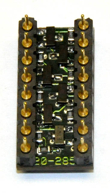
Having too much fun to give up, I bit the bullet and spent $100 for four-layer boards (two layers plus a power plane and a ground plane.) This greatly simplified the layout and allowed all my traces to be reasonably short. It also came with a solder mask, which solved the problem of my headers shorting to traces. When I powered my first prototype up (with the 1 GHz BFS17 transistors) it worked and I was able to get the instrument to pass its performance test with flying colors even without any recalibration! The working example is shown below.
Despite meeting all specifications, my reproduction is not as good as the original:
– There are still parasitic frequencies in the output but they are down ~70dB
– It is not as fast as the original – the output starts to drop off at about 110MHz while the original will go to over 111MHz (as fast as the oscillator in the pulse generator will go) with no signs of the output amplitude decreasing. That said in use it only ever sees signals as fast as 105MHz, so this is not really a problem.
– The input impedance is slightly different then the original so it may be necessary to perform calibration after replacing the part. In my case, however, it worked as-is.
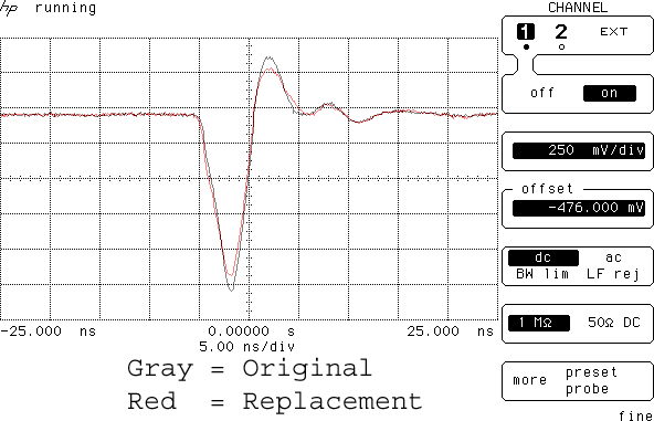
– The output pulse shapes are close to, but not exactly the same as, the original. The positive output pulse is pretty darn close, but the negative one is slightly lower in amplitude. See the output waveforms below. (The red trace is my replacement, gray trace is the original)

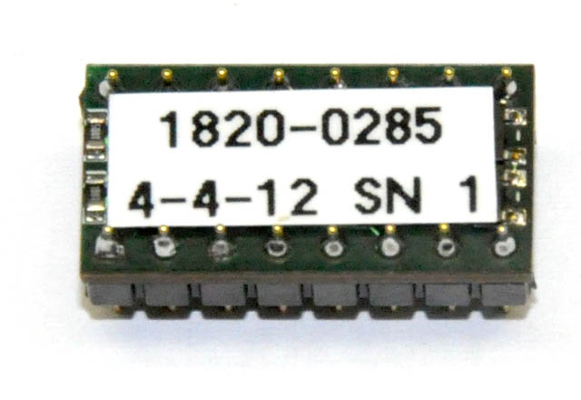
This was such a rewarding experience that I am planning on trying to replicate other ICs and hybrids used in vintage HP equipment using the same techniques. I will keep you all posted. As far as I know the part (HP 1820-0285) was used only in the 8007A and 8007B pulse generators, but I would love to hear about it if anyone finds another application.
The reproduction pulse shaper ICs are available for sale here.
Finally, here is a picture of the part installed in my generator. Note the shiny gold – they really don’t make ‘em like they used to…

-Matthew
Note that this post has been copied from:
http://www.antiqueradios.com/forums/viewtopic.php?t=190955
The publication date has been modified to reflect the original posting date.
Great story & congrats!